Senior Data Scientist
It is estimated that by the year 2030, approximately 20 percent of the whole world’s energy consumption will be attributed to the ICT sector. A major contributing factor is the semiconductor industry, in other words producing microchips, which has not only surpassed the car industry as a major polluter, but also consumes water at huge rates. More than 80% of semiconductors are produced in Korea and Taiwan, where lack of water resources, for example, have hindered the production of microchips.
Semiconductor plants are usually called fabs, and the electricity used in the fabs is 40–50% due to manufacturing and 50–60% due to maintenance and infrastructure. The whole electricity use in a fab is up to 100 MWh per hour, and it includes for example air filtering and ventilation, water treatment, and the use of tools such as plasma-etching torches.
The sustainability problem created by semiconductor fabrication is manyfold, as the creation process for each new generation of microchips requires more energy and water, and the carbon footprint of the industry is already gigantic. For example, roughly a third of the CO2 emissions of the ubiquitous Apple iPhone is from microchip production.
At the same time, there is a global shortage of semiconductors. Even before the pandemic, demand exceeded supply, but Covid-19 made the situation considerably worse. The industry has to tackle two problems at the same time: propping up production while making the process more sustainable.
Some may question if the semiconductor industry can ever reach sustainability at a reasonable level. However, chips are needed to produce solar panels and other green technologies we have developed to combat the looming climate catastrophe. Their need is undeniable in that sense, in addition to semiconductors being essential components in every electronic device we use in our everyday lives.
Fortunately, as we are reaching Industry 5.0, we are also on the brink of a solution for implementing more powerful Statistical Process Control (SPC) systems to increase yield and reduce scrap rate in fabs. This direction towards sustainability is made possible by Artificial Intelligence and Machine Learning.
Here Be Deviations
The essential thing in enhancing semiconductor manufacturing and making it more sustainable is the production of Integrated Circuits (IC) on the silicon wafers. Wafer is a thin slice of semiconductor made from crystalline material that acts as the substrate for microelectronic devices built upon it.
Because the manufacturing process of an IC is extremely complicated, consisting of more than hundred process steps and taking up to four months in time, a huge amount of data is collected in their production. That is in order to enable early detection of production failures so that the yield of an individual wafer can be maximised.
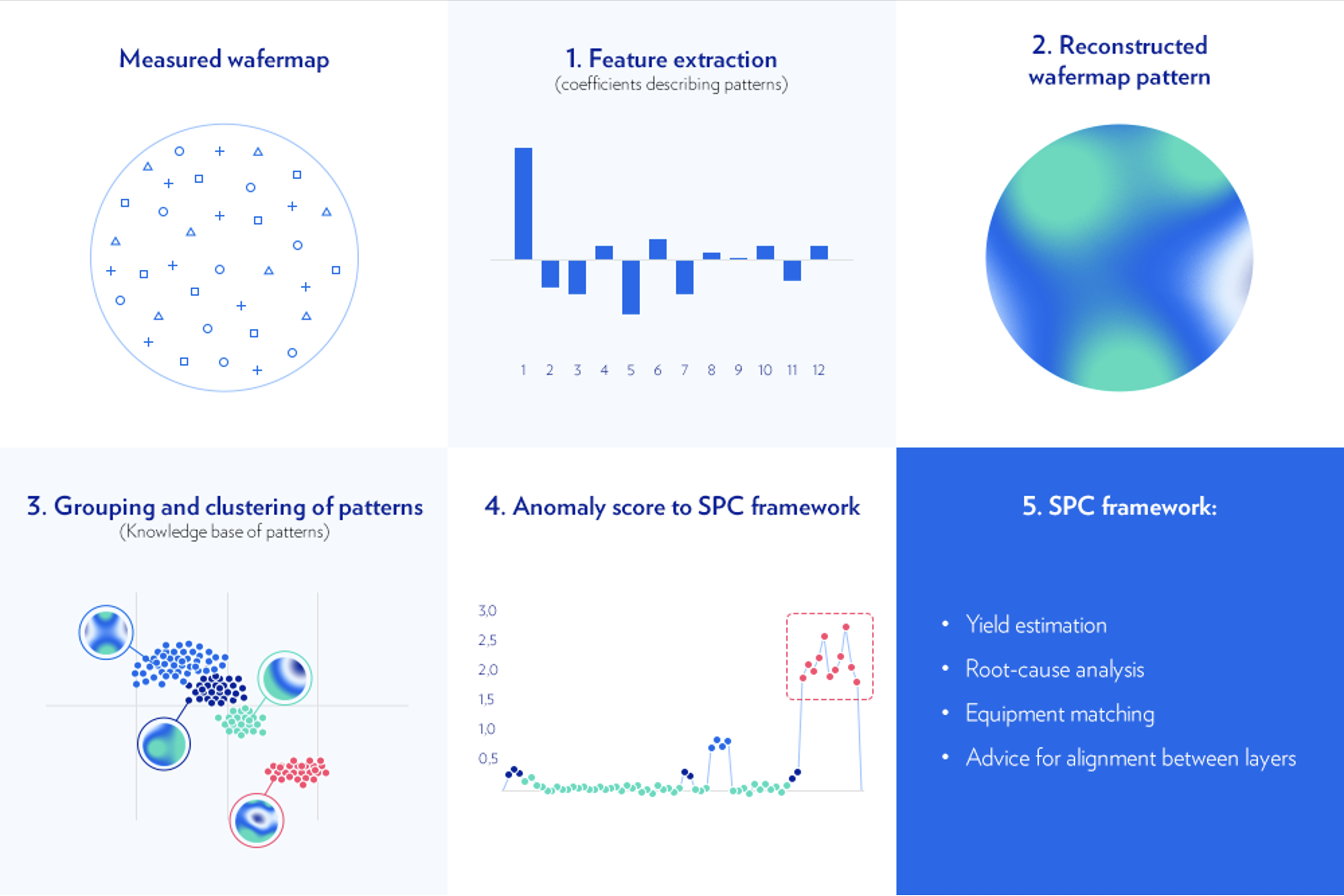
The collection of wafer data and portraying their spatial characteristics is called wafer mapping. A wafer map is created by taking measurements of specific surface points of a wafer, and the map shows the uniformity of the surface and how much it deviates from the ideal. The traditional analysis of the wafer profile is based on summary statistics and sampling measurements.
Wafer mapping is an important part of SPC, but it has its unquestionable limitations. In addition to information loss when using summary statistics, it cannot be used to distinguish different shapes such as convexity and concavity from each other, or alternatively to alarm when the radial symmetry of the wafer profiles is violated.
Mapping is also very product-specific and getting accurate results depends on the chip dimensions – the location, shape, and sharpness of variation patterns cannot be detected, and comparison of profiles over different product types is not possible.
The overall stability of the manufacturing process and the detection of Out-of-Control signals in semiconductor fabs is traditionally based on control charts, such as EWMA charts (exponentially weighted moving average charts) and Shewhart’s charts, which monitor process variables and attributes and ensure they stay within given limits. The data provided is very limited and doesn’t contribute to intelligently enhancing the process.

This is where AI/ML solutions come in. By using them, it is possible to gain understanding of spatial profiles over the entire product portfolio and use it to adjust the production process when a defective or anomalous product is detected. AI/ML methods enable improved pattern and shape recognition when it comes to complex data formats such as time series or images, which are beyond the limits of even the most advanced systems in place at the moment.
Onward from Basic SPC Solutions
An AI/ML-based solution that we have come up with is a so-called Critical Profile Detector. Real-time online AI analysis is integrated into a SPC framework to drive intelligent decision-making and make automated corrective actions to enhance productivity.

Critical Profile Detector is very Industry 5.0, as it is built on the notion that humans and machines collaborate within a digital ecosystem. AI and ML allow optimising the process without human intervention but empower humans with smart solutions, maximising efficiency and productivity and thus making the process more sustainable. The solution also provides a competitive advantage to semiconductor fabs from competitors still using basic SPC solutions.
There are three aspects to this solution: explainability and interactivity, which lead to intelligent actions to correct the process.
Explainability comes down to Machine Learning algorithms that analyse the data flow and detect process deviations and anomalies from data formats and flows. A human observer wouldn’t necessarily be able to spot the deviations and anomalies. In addition, the algorithm converts the results to the user interface in a clear form.
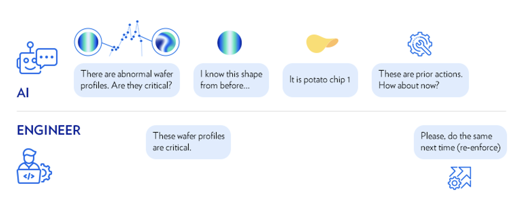
Interactivity allows the process expert to decide which anomalies are critical, based on the AI model data, whereas Intelligent actions are based on the power of AI. AI is able to make connections between expert insights of incidents that occurred in history and predict their occurrence in the future.
Furthermore, the process can be refined into automated actions using Out-of-Control Action Plan (OCAP) process which is seamlessly integrated with the real-time AI/ML analysis.
AI-assisted analysis includes all process data from numerical information to operational components such as the equipment used. Using multivariate discriminant analysis, AI is able to find the highest contributor to the Out-of-Control action, in other words, the root cause of the problems. As the AI learns the wafer profiles, the OCAP processes will get more and more accurate and efficient.
Better Productivity Through Artificial Intelligence
The specific SPC framework we are offering for Critical Profile Detection is called LineWorks SPACE and its add-on eCAP (Electronic Corrective Action Plan) which enables powerful AI/ML solutions. LineWorks SPACE acts as the data source for all measured data, from product quality, to equipment sensor data. Its ecosystem consists of various chart plug-ins and add-ons.
SPACE eCAP add-on integrates the whole wafer production process with AI/ML algorithms that make it possible to develop machine learning models and enhance productivity through automatic corrective action plans. Anomaly detection, prediction of system performance, process deviations, and other pertinent data is gained not on only single steps in the process but of the entire manufacturing chain at different product lines.With eCAP the system is also capable of reacting to observed deviations through intelligent corrective actions.
By getting to the root causes of glitches in the process, AI/ML identifies the best course of corrective action and enables humans to make better decisions. Furthermore, you can implement real-time AI/ML scoring and enable engineers to trigger eCAPs whenever an anomaly is detected.
The AI learns the typical actions and decisions applied to all wafers having similar critical defective profiles and initiates eCAP processes immediately when an anomaly is detected, executing the same set of actions as in the past. If there is a combination of possible actions, human decision input will be requested, thus users can decide the appropriate corrective actions and design the execution accordingly.
By this Critical Profile Detection through AI/ML solutions we are able to greatly enhance semiconductor production, increase yield, and make the production processes in fabs more sustainable. As the future doesn’t show any signs of us using less microchips – on the contrary – these kinds of solutions become more and more important in building a sustainable future and combating the climate catastrophe efficiently industry-wide.

Kalle Ylä-Jarkko is working as a Senior Data Scientist in Elisa IndustrIQ and is developing AI/ML models for camLine’s flagship LineWorks SPACE for complex operational systems in manufacturing, telco, and semiconductor industries. Kalle has a long back-ground in start-ups in laser industry and he holds 6 patents and is the author of over 30 papers in the field of laser technology, laser machining, machine learning, and AI applications.
Sources
Alan Crawford, Ian King, Debby Wu: The Chip Industry Has a Problem With Its Giant Carbon Footprint (Bloomberg, 2020) – https://www.bloomberg.com/news/articles/2021-04-08/the-chip-industry-has-a-problem-with-its-giant-carbon-footprint
Udit Gupta, Young Geun Kim, Sylvia Lee, Jordan Tse, Hsien-Hsin S. Lee, Gu-Yeon Wei, David Brooks, Carole-Jean Wu: Chasing Carbon: The Elusive Environmental Footprint of Computing (2020)
Bryan Ng, Nils Knoblauch, Kalle Ylä-Jarkko, Rasmus Heikkilä: Machine Learning in an SPC Framework Drives Productivity (2022)
Future-Fit Heatmap: Semiconductor Manufacturing (Future-Fit, 2020) https://futurefitbusiness.org/wp-content/uploads/2020/09/Semiconductor-Manufacturing-Future-Fit-Heatmap.pdf